|
|
||
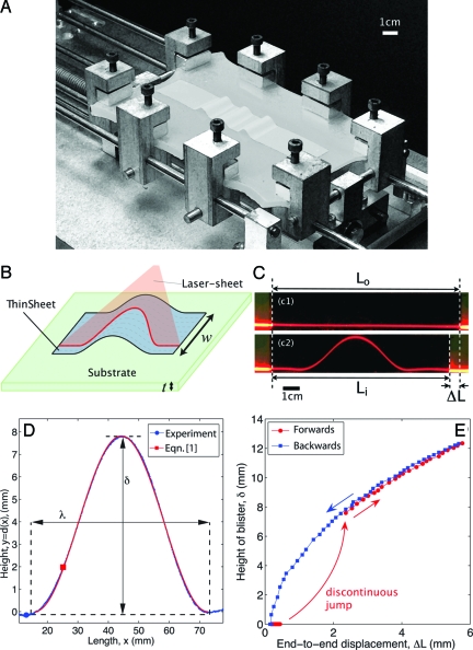
Macroscopic delamination blisters. (A) Macroscopic experimental setup for studying the delamination of thin films adhered to soft substrates. (B) A laser sheet is used to measure the profile of the blister(s) as the end-to-end compression ΔL is increased. (C) Plan views of the blister profile as shown by an oblique laser sheet just before (c1) and just after (c2) delamination. (D) Processing these images gives the blister profile y = d(x) (blue points), which is well fitted by the cosine form Eq. 1 (red curve). This fit gives the blister size λ and height δ. (E) Plot of the evolution of the blister height as ΔL is increased (red curve) and then decreased (blue curve). In A the film has thickness h = 50 μm, whereas for C–E, h = 90 μm.
From:
Dominic Vella, Jose Bico, Arezki Boudaoud, Benoit Roman and Pedro M. Reis, “The macroscopic delamination of thin films from elastic substrates”, Proc Natl Acad Sci USA, Vol. 106(27), 2009, DOI: 10.1073/pnas.0902160106
ABSTRACT: The wrinkling and delamination of stiff thin films adhered to a polymer substrate have important applications in “flexible electronics.” The resulting periodic structures, when used for circuitry, have remarkable mechanical properties because stretching or twisting of the substrate is mostly accommodated through bending of the film, which minimizes fatigue or fracture. To date, applications in this context have used substrate patterning to create an anisotropic substrate-film adhesion energy, thereby producing a controlled array of delamination “blisters.” However, even in the absence of such patterning, blisters appear spontaneously, with a characteristic size. Here, we perform well-controlled experiments at macroscopic scales to study what sets the dimensions of these blisters in terms of the material properties and explain our results by using a combination of scaling and analytical methods. Besides pointing to a method for determining the interfacial toughness, our analysis suggests a number of design guidelines for the thin films used in flexible electronic applications. Crucially, we show that, to avoid the possibility that delamination may cause fatigue damage, the thin film thickness must be greater than a critical value, which we determine.
Page 167 / 360