|
|
||
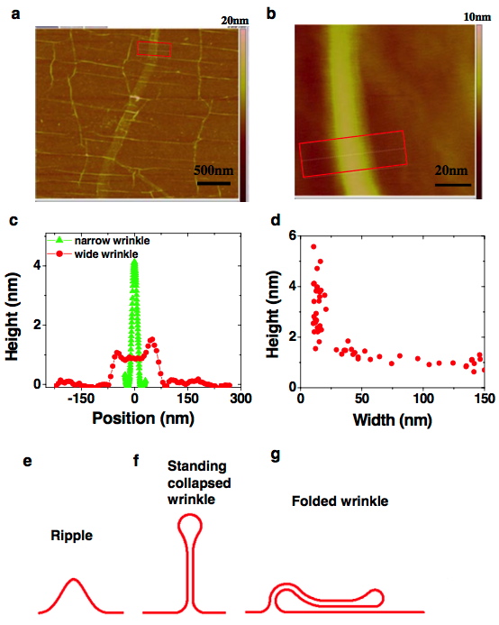
Figure 2. Wrinkle topographies and structures. (a) AFM image of graphene on SiO2/Si substrate. The field of view is 3 μm. (b) AFM image of a narrow wrinkle. Field of view is 100 nm. (c) The step profile of a wide and a narrow wrinkle. (d) Statistical distribution of wrinkle heights as a function of their width. Schematic illustration of three classes of graphene wrinkles: (e) simple ripple; (f) standing collapsed wrinkle; (g) folded wrinkle. For details on these geometries see the Supplemental Information.
From:
Wenjuan Zhu, Tony Low, Vasili Perebeinos, Ageeth A. Bol, Yu Zhu, Hugen Yan, Jerry Tersoff, and Phaedon Avouris (IBM Thomas J. Watson Research Center, Yorktown Heights, New York),
“Structure and electronic transport in graphene wrinkles”, Nano Letters, Vol. 12, No. 7, pp 3431-3436, 2012, DOI: 10.1021/nl300563h
ABSTRACT: Wrinkling is a ubiquitous phenomenon in two-dimensional membranes. In particular, in the large-scale growth of graphene on metallic substrates, high densities of wrinkles are commonly observed. Despite their prevalence and potential impact on large-scale graphene electronics, relatively little is known about their structural morphology and electronic properties. Surveying the graphene landscape using atomic force microscopy, we found that wrinkles reach a certain maximum height before folding over. Calculations of the energetics explain the morphological transition and indicate that the tall ripples are collapsed into narrow standing wrinkles by van der Waals forces, analogous to large-diameter nanotubes. Quantum transport calculations show that conductance through these “collapsedwrinkle” structures is limited mainly by a density-of-states bottleneck and by interlayer tunneling across the collapsed bilayer region. Also through systematic measurements across large numbers of devices with wide “foldedwrinkles”, we find a distinct anisotropy in their electrical resistivity, consistent with our transport simulations. These results highlight the coupling between morphology and electronic properties, which has important practical implications for large-scale high-speed graphene electronics.
Page 131 / 360